
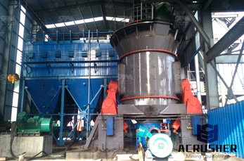
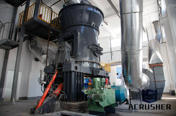
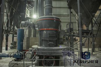
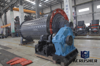
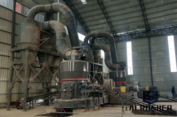
grinding process in mems manufacturer Grasping strong production capability, advanced research strength and excellent service, Shanghai grinding process in mems supplier create the value and bring values to all of customers.
 WhatsApp)
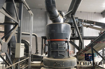
Failure modes of Wafer Level Thin Film MEMS packages during wafer thinning. ... of the grinding process. ... thin film packaging process for a MEMS cantilever type resonator using a 4mask ...
Study of Peck drilling of borosilicate glass with μRUM process for MEMS. ... micro electro mechanical systems. USM. stationary ultrasonic machining. RUM. ... They reported that cutting force could be reduced to about 50% and MRR could be improved to 10% as compared to diamond grinding process with RUM. MRR was found to be proportional to ...
A SICMOSMEMS process using backside grinding IEEE Xplore This paper presents a SiCMOSMEMS fabrication process which leaves the backside silicon under the CMOS metal and oxide layers, and improves the ...
・Built in edge trimming system is available as an option for thin wafer process. ・Dual index system, which polishing stage and grinding stage is completely separated, satisfy the cleanness required for TSV and MEMS process. ・Less than Ra1Å ultra luminance, ultra mirror surface is possible.
Micromachining: A New Trend in Manufacturing Prof. Farzin Heidari, Texas AM University, Kingsville ... turning and grinding process for a wide range ... and MEMS 2015 Manufacturing Technology Lab focused on Micro Electro Mechanical systems (MEMS) fabrication process control. Topics include fabrication processes related to
The process frequency can act as an actuator on any part of the MEMS. Depending on the geometry and materials of the MEMS under consideration, it is necessary to analyze to likelihood of problems. If one of the eigenfrequencies of the MEMS or the WLTFP is (very) close to the bonding frequency, it may start to resonate.
A SICMOSMEMS PROCESS USING BACKSIDE GRINDING Y.J. Fang 1, A. Wung 1, T. Mukherjee 1, and Fedder 1, 2, 3 1Department of Electrical and Comput er Engineering, Pi ttsburgh, PA, USA 2The Robotics Institute, Pittsburgh, PA, USA 3 Institute for Complex Engineered Systems, Pittsburgh, PA, USA ABSTRACT This paper presents a SiCMOSMEMS fabrication ...
MEMS Fabrication I : Process Flows and Bulk ... • Reader is in! (at South side Copy Central) • Kovacs, "Bulk Micromachining of Silicon," pp. 153643. • Williams, "Etch Rates for Micromachining Processing," pp. 25660. • Senturia, Chapter 3, "Microfabrication." • Today''s Lecture • Tools Needed for MEMS .
The field of materials and process integration for MEMS research has an extensive past as well as a long and promising future. Researchers, academicians and engineers from around the world are increasingly devoting their efforts on the materials and process integration issues and opportunities in MEMS .
MEMS Dicing. Dicing takes a finished wafer (postwafer fabrication) and converts it into individual dies; it''s the step where the frontend fab process transitions to the backend assembly process. Grinding Dicing Services, Inc. has accumulated 25 years of engineering and process knowledge supporting semiconductor, consumer electronics, and ...
Why dicinggrinding service by DISCO? DISCO HITEC EUROPE''s DicingGrinding Service (DGS) is an integral component of any manufacturing stage when it comes to high precision processing of ICs, MEMS, LEDs, other micro components and their inspection/metrology.
In the context of manufacturing integrated circuits, wafer dicing is the process by which die are separated from a wafer of semiconductor following the processing of the wafer. The dicing process can involve scribing and breaking, mechanical sawing (normally with a machine called a dicing saw) or laser methods are typically automated to ensure precision and accuracy.
The device for continuous gas density measurement in the process. Nanomass Gas Density is the first device for precise gas density measurement based on the revolutionary MEMSCoriolis technology – a combination of innovative microtechnology and Endress+Hauser''s long experience.
This application note discusses the Edge Grinding of hard, brittle materials that are common to semiconductor, MEMS, LEDs, and other applications. Edge grinding, also known as Edge Profiling, is a process that is common to the manufacture of nearly all semiconductor related
Products/Services for MEMS Grinding Polishing Buffs and Buffing Wheels (105 companies) Buffs and buffing wheels are used to hold finishing compounds and polish parts made of metal, plastic, ceramic, glass, wood, stone, silicon, or optical materials.
MEMS packaging accounts for 2060% of the MEMS device BOM and is a key part of the MEMS function and design Packaging creates additional value as the MEMS device is integrated into a system (SiP, module) Standardization enables high volume production (second sourcing, cost efficiency through technology sharing)
Meister Abrasives'' micro grit product range used for fine grinding of prime wafers or back thinning applications are capable of achieving surface finishes in the angstrom range. Ceramet hybrid and vitrified bonded grinding wheels create a quantum leap in photovoltaic grinding process .
The SiCMOSMEMS process includes a grinding process followed by a bonding process and conventional postCMOS etch. A SiCMOSMEMS accelerometer is used to demonstrate the feasibility of the SiCMOSMEMS process. A µm flatness of ground silicon surface over 2 .
Safe values for SOI thickness and cavity width during grinding of CSOI wafers. cavity breakage. For very thin diaphragms a combined grinding, etching and polishing process can be utilized. One application area for the CSOI wafers is RF MEMS Fig. 4. Microscopy image of .
MEMS, MOEMS, sensors and other devices will be designed and fabricated with Stealth technology as the preferred medium for final singulation or dicing. The addition of Stealth Laser Dicing services fortifies our line of mechanical saws, which has been the de facto dicing standard for decades.
5 Sensors and MEMS for IoT Edge Devices • Sensors convert environmental information to an electrical signal • Some sensors are MEMS based MEMS sensors are evolving at a rapid pace (size, function, cost) • MEMS devices for IoT Standard products/standard packages
Nanogrinding was performed based on a lapping process.[16] The abrasive grains were completely embedded in a soft metallic plate that was the grinding tool. Pumice was embedded in the grinding plate and remained there throughout the process. Between pumice particles, the basic soft metallicplate materials formed the plateaus.
Technologies like RFID, MEMS Devices, and power devices are considered to be the major source of demand for these thin wafers. This scenario is increasingly creating demand for a better manufacturing process, especially processing and dicing which are important phases of ultrathin wafer production. ... The grinding process in TAIKO leaves an ...
MEMS Journal: What are some of the main challenges with WLP right now? What needs to be solved and why? David Wilkie: Some of the main challenges in WLP today include thin wafer processing, handling of thin wafers using either temporary carrier technologies with minimal cost or the Taiko grinding process. The infrastructure available to support ...
WhatsApp)