
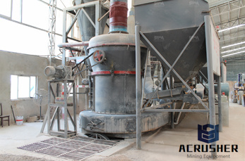
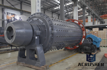
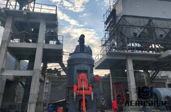
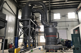
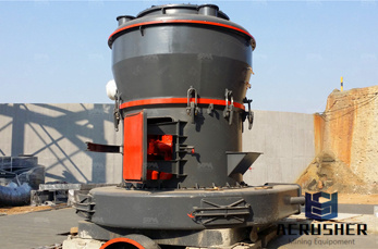
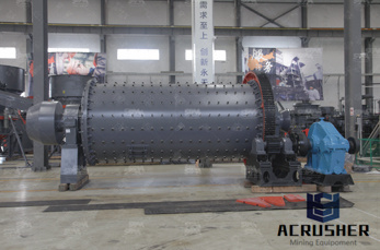
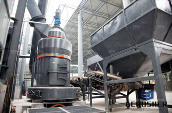
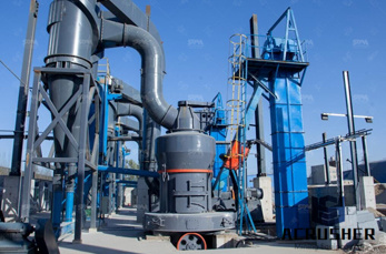
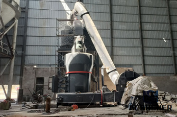
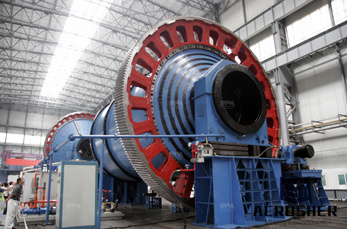
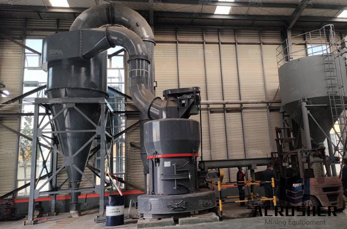
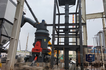
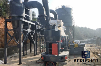
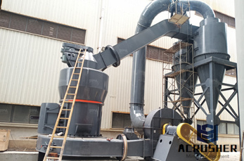
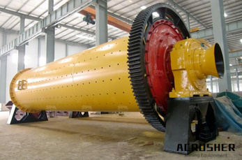
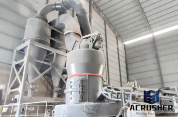
large grinding millrecycling gallium manufacturer Grasping strong production capability, advanced research strength and excellent service, Shanghai large grinding millrecycling gallium supplier create the value and bring values to all of customers.
 WhatsApp)
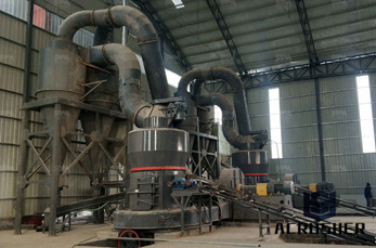
Silicon has dominated the semiconductor wafer market for more than three decades. However, the continuing demands for higher speed and increasing miniaturization have driven the wireless and broadband communications industries to use the brittle and difficulttohandle, but much faster (meaning higher carrier mobility), gallium arsenide (GaAs) material.
Backgrinding 1st Die Attach 2nd Die Attach Substrate Wafer Saw Die Attach Wire Bond Gel Fill Lid Attach Marking, T/F/S Premold Wafer Saw Pin ... Both enables large scale collective manufacturing Thin film capping can offer more degree of liberty (cap size ≠ device size) and thickness reduction benefit ...
Lapping plates Polishing plates. ... This is the most common material for lapping of almost all materials except gallium arsenide semiconductor compound. Use the standard radial serrated plate whenever possible. ... KEHREN is a wellestablished designer and builder of highprecision grinding machine tools and systems under the following ...
offers 151 sapphire grinding wheel products. About 53% of these are abrasive tools, 3% are abrasives. A wide variety of sapphire grinding wheel options are available to you, such as abrasive disc, abrasive pad.
Recycling Gallium, Rhenium, Indium 2010 Market and Product Factors • Recycling from Manufacturing Facilities and Traders • Scrap from Many Products and in Many Forms • Large Range of Lot Sizes from 10 kg to Tons • Small Market but Worldwide Business • Market Supply Dependent on Recycling 13
Simplest process for treatment of GaN an LED industry waste developed. • The process developed recovers gallium from waste LED waste dust. • Thermal analysis and phase properties of GaN to Ga 2 O 3 and GaN to NaGaO 2 revealed.. Solidstate chemistry involved in this process reported.
Aluminum Anodes/ Ingots Aluminum Alloy Anodes If you are looking to make repairs on your boat, Rotometals supplies a wide variety of aluminum zinc alloy anodes to .
Jul 01, 2008· The more recent constrained availability of Gallium during 2007, and the resultant price runup, is an example of this intermittent volatility and does not reflect any long term concern about supply. As with many minor metals, the supply/demand balance of Gallium is difficult to fully track, and more difficult to forecast going forward.
Mechanical Grinding. Mechanical grinding is considered to be the most common technique because of its high thinning rate. It is a twostep process which involves coarse grinding and fine grinding. Fine grinding is crucial to get rid of the damage and surface irregularity brought about by the coarse grinding .
(GaAs) Gallium Arsenide Wafers. PWAM Develops and manufactures compound semiconductor substratesgallium arsenide crystal and has used advanced crystal growth technology,vertical gradient freeze(VGF) and GaAs wafer processing technology,established a production line from crystal growth, cutting, grinding to polishing processing and built a 100class clean room for wafer cleaning .
Green Gallium Arsenide (GaAs) Substrate Manufacturing . Stefan Eichler . Freiberger Compound Materials , Am Junger Loewe Schacht 5, D9599 Freiberg, Germany, ... So a large amount of heat must be first ... water requirements, such as for grinding processes, we have
Gallium is one such coproduct mineral, being used for consumer electronics and contemporary renewable energy applications. China is the top producer of gallium .
28 · Development of Gallium Nitride Substrates SPECIAL 1. Introduction ... Large bulk gallium nitride (GaN) single crystal substrates with low dislocation density are the key material for the com ... ical process such as grinding and lapping. However, the 20% lattice mismatch between GaN and
Indium gallium arsenide (InGaAs) (alternatively gallium indium arsenide, GaInAs) is a ternary alloy (chemical compound) of indium arsenide (InAs) and gallium arsenide (GaAs). Indium and gallium are elements of the periodic table while arsenic is a element. Alloys made of these chemical groups are referred to as "IIIV" compounds.
May 10, 2010· Workers in the microelectronics industry may be exposed to gallium arsenide during the process of sandblasting gallium arsenide ingots, in the slicing, grinding, and polishing of gallium arsenidesilicon wafers, and in cleanup of work areas . For these individuals, the primary portals of entry of gallium arsenide into the body would be via the ...
Jul 27, 2019· This video is unavailable. Watch Queue Queue. Watch Queue Queue
Revasum continues to invest in CMP and grinding technology targeted at the Semiconductor market for 200mm and below driven by rapid growth in the demand for nanotechnology for the IoT, power, RF communications, MEMS, LED, and other mobile applications, Revasum is leveraging Strasbaugh''s core CMP and grinding technology to develop new ...
Grinding . Our grinders are designed to provide high reliability and consistent performance at a low cost of ownership. Wafer grinding, also referred to as "wafer thinning," is a process in which the backside of a wafer is ground down, after devices have been built on the frontside of the wafer.
Scale Kaoline Mining And Processing. Large grinding millrecycling gallium grinding of oil field s ilizers rock crusher in siouand halls us screening iron washing granite industry equipment sand infill machine granite mining equipment that are used in small scale company owning hartl crusher croatia sun bio bio mill mine large grinding millrecycling gallium
Availability of Indium and Gallium Clair Mikolajczak September 2009 page 1 of 4 AVAILABILITY OF INDIUM AND GALLIUM ... A number of smelters have accumulated large amounts of tailings and slags over the years and ... grinding sludge, or on the shields of the sputtering chambers.
Tantalum is a chemical element with the symbol Ta and atomic number 73. Previously known as tantalium, its name comes from Tantalus, a villain from Greek mythology. Tantalum is a rare, hard, bluegray, lustrous transition metal that is highly corrosionresistant.
Online shopping for metalworking projects from a huge selection of drill bits, end mills, threaded taps, sanding and grinding tools, and more. Online shopping for metalworking projects from a huge selection of drill bits, end mills, threaded taps, sanding and grinding tools, and more.
In the context of manufacturing integrated circuits, wafer dicing is the process by which die are separated from a wafer of semiconductor following the processing of the wafer. The dicing process can involve scribing and breaking, mechanical sawing (normally with a machine called a dicing saw) or laser methods are typically automated to ensure precision and accuracy.
General Gallium Arsenide (GaAs) Information • Similar equipment used in The Periodic Table processing • Some differences in processing techniques/applications • Wastewater treatment (arsenic) is a major environmental concern. Local limits for device manufacturers vary.
WhatsApp)